
The purpose of this document is to provide guidelines and some example implementations for the integration of safety-certified drives, such as the Everest S Safe NET and Denali Safe NET, in compliance with the applicable safety requirements (the Safety Manual of EVS-S-NET-E and of DEN-S-NET-E). Although these drives are safety-certified, achieving a safety-compliant system depends not only on the drive itself but also on its correct integration into the final application.
When designing an interface board, one of the fundamental questions to address is: What can fail in the system, and how can a hazardous or catastrophic failure be prevented? This does not imply that component failures can be entirely eliminated. Instead, the objective is to strategically implement monitoring and protection mechanisms that prevent faults from propagating to the drive, causing it to operate outside its specified limits and potentially resulting in unexpected or unsafe behavior.
For this reason, every circuit block should be evaluated in relation to the drive signals it interfaces with. The integration requirements associated with each drive input and output must be carefully reviewed to ensure that all failure conditions remain within the permissible limits defined by the drive specifications.
Although the concept is straightforward, its implementation can be challenging in practice due to space constraints, system complexity, and the detailed failure-mode analysis required to verify compliance with the specified electrical and safety requirements.
Failure to meet these integration requirements may compromise the functional safety performance of the overall system, regardless of the safety certification of the drive. Consequently, it is the responsibility of the system integrator to verify that the complete application satisfies all applicable safety requirements and certification objectives.
The parts of an interface board that are directly related with safety and are with more detail explained in this chapter are:
-
Voltage monitors
-
Supplies
-
Network Interface
-
Safe Inputs
-
Safe Outputs (only present in the EVS-S-NET drive)
-
Safe Outputs Diagnostic
-
Feedback Interface
Safe Brake Control circuitry are not implemented on the provided safety-drive integration boards. The client must therefore implement the required safety circuitry externally and ensure that the complete application complies with all applicable functional safety requirements.
Supplies
Power supply
The drive requires a 48 V SELV supply, with an operating range of 8 V to 60 V and a maximum fault voltage of 60 V. While the EVS-S-NET can withstand brief transients slightly exceeding 60 V without sustaining damage, its safety integrity cannot be assured under such conditions. Therefore, the system shall be designed to prevent overvoltages above 60 V during operation. This voltage limit is defined by certification requirements. For more information check the general section of the application guide, check out this link.
Voltage monitors
Voltage-monitoring circuits can generally be classified into two categories:
-
The first category consists of voltage supervisors that continuously monitor the supply voltage and provide a diagnostic signal, fault indication, or status output whenever the voltage exceeds or falls below predefined thresholds. These devices perform a monitoring function only and do not directly interrupt the power path.
-
The second category consists of protective voltage-monitoring circuits, which are placed in the power path or are capable of controlling a series disconnect element (such as a MOSFET, relay, or safety switch). When an overvoltage or undervoltage condition is detected, these circuits actively isolate or shut down the affected supply, preventing the fault from propagating to downstream safety-related components.
The selection of either approach depends on the required safety architecture, fault-response strategy, and the level of protection needed for the application.
5 V supply
The selection and implementation of the 5 V DC-DC converter responsible for generating the 5 V rail from the 60 V supply are left to the system designer. From a safety perspective of EVS-S-NET , the 5 V supply shall be distributed throughout the system and appropriately monitored to ensure that any fault affecting the logic supply keeps the voltage within the limits specified by the drive integration requirements for the respective conneced nets.
Please note that the 5 V input of the DEN-S-NET drive is not safety-related. Instead, the safety-related logic 3.3 V supply shall be designed, monitored, and supervised according to the same criteria described for the 5 V supply of the EVS-S-NET. Applying these requirements is necessary to ensure compliance with the functional safety requirements of the system.
Several architectural approaches may be adopted depending on the system design. As an example, this guide classifies the distribution of the 5 V rail into three categories: non-safe circuits, internal safety-related circuits, and external safety-related circuits. The distinction between safety-related and non-safety-related circuitry is entirely dependent on the application and the safety architecture adopted by the system designer.
The following table provides a simplified overview of these categories. For detailed requirements, including fault reaction times, diagnostic coverage, and safety integrity constraints, always refer to the Safety Manual of the selected drive.
|
5 V rail name in the described example |
Circuit category |
Possible use-case scenario |
|---|---|---|
|
+5V_PROT |
Non-Safe Circuits
|
This branch can be used for the motor temperature sensor interface, Ethernet link status LED drivers, GPIOs, and other auxiliary monitoring or indication circuits that do not represent any realtionship to the safety aspect of the final application. |
|
+5V_SAFE |
Internal Safety-related circuits.
|
This supply rail can be used to power feedback sensors, the safe input interface, or any other safety-related circuitry whose signals are ultimately processed by the drive. |
|
+5V_SOUT |
External Safe-related circuits.
|
This supply rail is intended to power interface circuits associated with the drive's safe outputs, as well as other external components that, despite being located outside the drive, are considered part of the safety-related system. |
Each category is intended to be protected and supervised independently to ensure compliance with the minimum and maximum allowable voltage limits under both normal and fault conditions, while preventing fault propagation between the different circuit domains supplied by each branch. A thourough analyis of Failure Modes and Effects Analysis is required.
The following selected nets can serve as idea of what aspects to be taken into account when selecting the voltage monitor. These nets may be either directly connected to the corresponding supply rail or interfaced through intermediate circuitry. In either case, the type of failures considered toghether with the maximum allowable voltages of this nets have a direct relationship to modeling the limits evaluated by the voltage monitor. Respecting these limits is crucial as it guarantees a failure in safe state.
|
Relevant safety nets |
Maximum nominal voltage |
Maximum voltage in the event of an external failure |
|---|---|---|
|
5 V Feedback supply sense
|
6.5 V |
25 V |
|
3.3 V Feedback supply sense
|
3.5 V |
25 V |
|
Absolute encoder 1 and 2 lines
|
3.5 V |
5.5 V |
|
Quadrature Incremental Encoder lines
|
3.5 V |
5.5 V |
|
Digital Halls lines
|
3.5 V |
6.5 V |
|
Safe inputs
|
6 V |
25 V |
|
Safe outputs (only for EVS-S-NET)
|
3.5 V |
25 V |
|
Safe outputs diagnostics (only for EVS-S-NET)
|
3.5 V |
6.5 V |
EXAMPLE SCENARIO: The general 5 V bus is routed through a protective voltage-monitoring circuit, whose output is limited to 6.5 V in the event of a DC-DC converter failure. The protected supply is designated +5V_SAFE. The external feedback sensors are powered from the +5V_SAFE rail, while the associated transceiver circuitry is supplied by the +3.3V_SAFE_EXT output provided by the drive, which is described in more detail in the following chapter.
Under normal operating conditions, the nominal input-voltage limits of the post-transceiver signals (the signals entering the drive) are inherently respected by the drive circuitry providing the +3.3V_SAFE_EXT supply. However, the signals that travel from the feedback connector inputs toward the transceiver are referenced to the +5V_SAFE rail.
In the event of a 5 V DC-DC converter fault, the feedback sensor signals are no longer referenced to the expected 5 V but instead to the voltage-monitor limited output, which is 6.5 V.
Depending on the capabilities of the selected transceiver, this increase in the signal voltage level originating from the sensors may be tolerated, allowing correct operation to be maintained.
If this is not the case, a worst-case scenario would occur in which the excessive voltage applied to the sensor signals causes the transceiver to short the sensor-side signals to the drive input signals. As a result, the drive feedback-input channels could be directly exposed to 6.5 V.
When checking the maximum voltage under an external-failure condition for the digital Hall inputs, 6.5 V still guarantees a safe state and a predictable failure mode. However, for both absolute encoder and incremental encoder inputs, the maximum allowable voltage under an external-failure condition is 5.5 V. Therefore, the integration requirements are not fulfilled, and the drive behavior can no longer be guaranteed.
Consequently, the interface board design must ensure that the voltage presented to the drive inputs and outputs never exceeds the specified maximum voltage under external-failure conditions. When implementing the voltage-monitoring circuitry, the primary consideration is not the nominal operating voltage, but rather the maximum voltage that could be applied to these channels under fault conditions.
NOTE: The 5V_FBK_SENSE pin serves as measurement for the choosen 5 V supply provided to the feedback sensors. Between this monitoring pin and supply net, a 2.4 kΩ ±1%, ≥50 mW series resistor shall be connected. Not fulfilling this requirement implies that the safe drive will not operate correctly.
Schematic
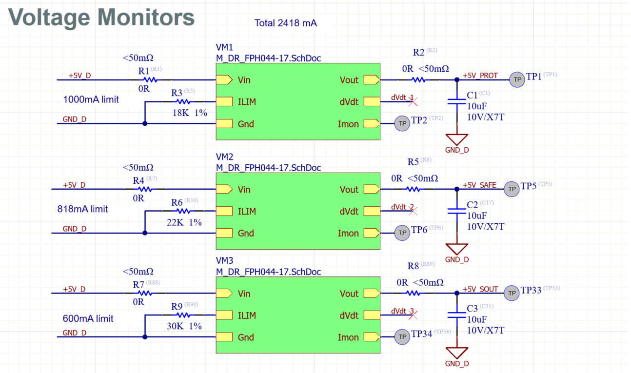
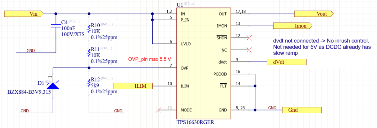
The suggested protective voltage-monitoring circuit was developed to satisfy the most stringent maximum voltage limits, ensuring a common design can be applied consistently to all three 5 V branches mentioned above. The only difference is the overload limit that has been computed based on the components connected to the design.
|
|
Signals description
|
Signal |
Description |
EVS-S-NET-E pins |
DEN-S-NET-E pins |
|---|---|---|---|
|
+5V_D |
5 V rail coming from the 5 V DCDC converter. |
- |
- |
|
+5V_PROT |
5 V rail destined for the non-safe circuits |
- |
- |
|
+5V_SAFE |
5 V rail destined for the internal safe circuits. Connected to the feedback connector to serve as power supply for the feedback sensors.
|
|
|
|
+5V_SOUT |
5 V rail destined for the external safe circuits |
- |
- |
|
dVdt_1 |
A capacitor from this pin to GND sets output voltage slew rate. Leaving this pin floating enables device power up in thermal regulation resulting in fast output charge. |
- |
- |
|
dVdt_2 |
|||
|
dVdt_3 |
|||
|
GND_D |
Ground reference. |
Pin 41 connector P3 |
Pin 31 connector P3 |
Design Notes
-
Vin ranges from 4 V to 60 V. It is important for it to be tolerant to 60 V to be prepared of a failure in the 5 V DCDC that would short-circuit the 5 V rail with the power supply.
-
Minimum OV, worst case: 5.14 V and Maximum OV, worst case: 5.497 V. The OVP values come from the resistor divider ratio and the ±2% OVP comparator accuracy.
-
This voltage monitor has a very low Rdson but using the UVLO pin so it is not able to set a undervoltage threshold at 4.5 V. Therefore, it was decided to NOT use the UVLO pin and only use the internal POR as undervoltage detector at 4.2 V aprox. UVLO values come from the UVLO threshold added to the minimum and maximum effective Zener voltage used in the worst-case analysis. UVLO_falling_worstcase = 4.116 V and UVLO_rising_worstcase = 4.386 V.
-
ILIM in each branch was set differently as to reflect the required overload limit of each branch (IOL = 18 / RILIM).
-
The output voltatge slew rate was not set, but bear in mind that it can be set by placing a capacitor from pin dVdTX to GND. For more information check the TPS1663x datasheet.
Bill of materials
|
Designator |
Part Number |
Manufacturer |
Package |
Value / Description |
|---|---|---|---|---|
|
C1, C2, C3 |
GRM188D71A106MA73D |
Murata |
0603 |
Ceramic capacitor 10 µF, 10 V, X7T. |
|
C4 |
CGA3E3X7S2A104K080AB |
TDK Corporation |
0603 |
Ceramic capacitor 100 nF, 100 V, X7S. |
|
R1, R2, R4, R5, R7, R8 |
ERJ-2GE0R00X |
Panasonic |
0402 |
Jumper resistor 0 Ω, <50mΩ tolerance, -55°C ~ 155°C. |
|
R3 |
RC0402FR-0718KL |
Yageo |
0402 |
Resistor 18 kΩ, 1% tolerance, 1/16W. |
|
R6 |
CRCW040222K0FKED |
Vishay dale |
0402 |
Resistor 22 kΩ, 1% tolerance, 1/16W. |
|
R9 |
MC00625W0402130K |
Multicomp |
0402 |
Resistor 30 kΩ, 1% tolerance, 1/16W. |
|
R10, R11 |
RNCF0402BTE10K0 |
Stackpole Electronics Inc. |
0402 |
Resistor 10 kΩ, 0.1% tolerance, 0.1W, 25ppm. |
|
R12 |
RT0402BRD075K9L |
Yageo |
0402 |
Resistor 5.9 kΩ, 0.1% tolerance, 0.1W, 25ppm. |
|
U1 |
TPS16630RGER |
Texas Instruments |
24-QFN |
Voltage Monitor, OV UV OC. 60 V tolerant. |
|
D1 |
BZX884-B3V9,315 |
Nexperia |
SOD-882 |
Zener diode, 3.9 V nominal, ±2% tolerance, 250 mW continuous power, 40 W peak surge power. |
3.3 V supply
The 3.3 V supply input represents a key distinction between the EVS-S-NET and DEN-S-NET drives. The EVS-S-NET provides only a 5 V supply input (pins 7, 8, 9, and 10 of connector P4), whereas the DEN-S-NET provides both a 5 V supply input (pin 58 of connector P2) and a 3.3 V supply input (pin 23 of connector P2).
From a functional safety perspective, the safety-related supply differs between the two drives. For the EVS-S-NET, the 5 V supply input is safety-related. In contrast, for the DEN-S-NET, the 3.3 V supply input is safety-related, while the 5 V supply input is not.
Consequently, not only should an analysis similar to that described in the previous section be performed to verify that the selected solution satisfies the required voltage limits at the drive side, but the design must also ensure compliance with the safety requirements applicable to the 3.3 V supply rail. The 3.3 V supply shall remain within ±3% of its nominal value (3.20 V to 3.40 V under normal operating conditions) and shall not exceed 25 V under an external-failure condition.
The selection and implementation of the DC-DC converter responsible for generating the 3.3 V rail are left to the system designer.
3.3 V safe supply
For the EVS-S and DEN-S drives, a dedicated 3.3 V power-supply output is provided by the drive and may be used to power circuitry on the interface board, provided that the total current consumption does not exceed 150 mA. If a higher current is required, an external 3.3 V power supply must be implemented. In such cases, depending on the selected 5 V monitoring scheme and the architecture of the external supply, a dedicated voltage-monitoring circuit may be or not required to ensure compliance with the safety requirements of all powered components and to guarantee the reliable detection and handling of supply faults (check the limits in the bellow table).
This supply is mainly thought to power the feedback transceivers. Regardless of whether the transceivers are powered from the drive's 3.3V_SAFE_EXT output or from an external 3.3 V supply, the 3.3V_FBK_SENSE pin shall be connected to the same supply rail to enable proper monitoring of the feedback-interface supply voltage.
|
Signal |
Description |
EVS-S-NET-E pins |
DEN-S-NET-E pins |
Maximum nominal voltage |
Maximum voltage in the event of an external failure |
|---|---|---|---|---|---|
|
3.3 V safe power supply output
|
3.3 V safe power supply output. Has internal protection of over-current, over-voltage, under-voltage and reverse current. |
Pin 14 of the Interface connector P4. |
Pin 29 of the Interface connector P2. |
3.3V + 5% |
5.5 V |
|
3.3 V Feedback supply sense
|
Analog input for sensing the 3.3V Feedback Supply. If 3.3V_SAFE_EXT is used, it is recommended to connect 3.3V_SAFE_EXT to 3.3V_FBK_SENSE. |
Pin 40 of the Interface connector P4. |
Pin 33 of the Interface connector P2. |
3.5 V |
25 V |
Network Interface
The system shall provide an interface for two MDI differential-pair ports (one for the input port 0 and other to the output port 1) supporting 100BASE-TX Ethernet, implemented with either external magnetics or capacitive coupling on the interface board. Detailed examples of implementation can be encountered in the general schematic tips within the application guide.
Safe Inputs
Safe redundant inputs are highly application-dependent, as their implementation is closely related to the source and characteristics of the safety signal. The signals routed from the interface board to the drive shall comply with the voltage, current, and timing requirements specified for the safe inputs (refer to the safety manuals of EVS-S and DEN-S for detailed specifications).
In the EVS-S-NET and DEN-S-NET drives, the safety-rated inputs are of general purpose and can be configured by the Safety Master to the activate the desired safety function, such as STO or SS1-t, through the certified safety configuration. Therefore, they should not be treated as simple STO enable lines, but as part of the drive’s safety-control architecture and its corresponding integration requirements.
|
Signal |
Description |
EVS-S-NET-E pins |
DEN-S-NET-E pins |
Maximum nominal voltage |
Maximum voltage in the event of an external failure |
|---|---|---|---|---|---|
|
\SAFE_INPUT_A |
Channel A of the redundant Safe Input 1. Active with low-level or open-circuit. |
Pin 33 of the Interface connector P4. |
Pin 13 of the Interface connector P2. |
6 V |
25 V |
|
\SAFE_INPUT_B |
Channel B of the redundant Safe Input 1. Active with low-level or open-circuit. |
Pin 34 of the Interface connector P4. |
Pin 17 of the Interface connector P2. |
6 V |
25 V |
In addition, before being connected to the drive, each safe input must implement the mandatory input-conditioning architecture shown below. This network consists of an overvoltage protection on the board inputs signals, a 220 Ω series resistor and a 7.5 kΩ pull-down resistor to GND, which shall be placed according to the recommended diagram. Compliance with this requirement is mandatory to ensure correct operation and validation of the safe input circuitry.
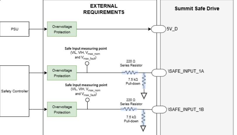
All safe-input signals implemented on the interface board are recommended to be sourced from the +5V_SAFE branch of the logic supply. This dedicated safety supply rail ensures that the safe-input circuitry operates within the required safety constraints and remains electrically independent from non-safety-related logic circuits.
Safe Outputs (EVS-S-NET only)
The implementation of redundant Safe Outputs, similarly to Safe Inputs, is highly dependent on the end application and can be realized in a variety of ways. In many applications, these signals are used for safe brake control, although other functions, such as system enable signals, status indication, or the activation of safety-related circuitry, may also be implemented.
However, their use is not limited to local circuitry. When required by the application, the Safe Outputs may also be used to drive external safety-related devices, provided that the overall safety architecture and functional safety requirements are maintained.
The Safety Core is the one controlling the Safe outputs.
Regardless of the specific application, the interface board shall comply with the following mandatory integration requirements:
-
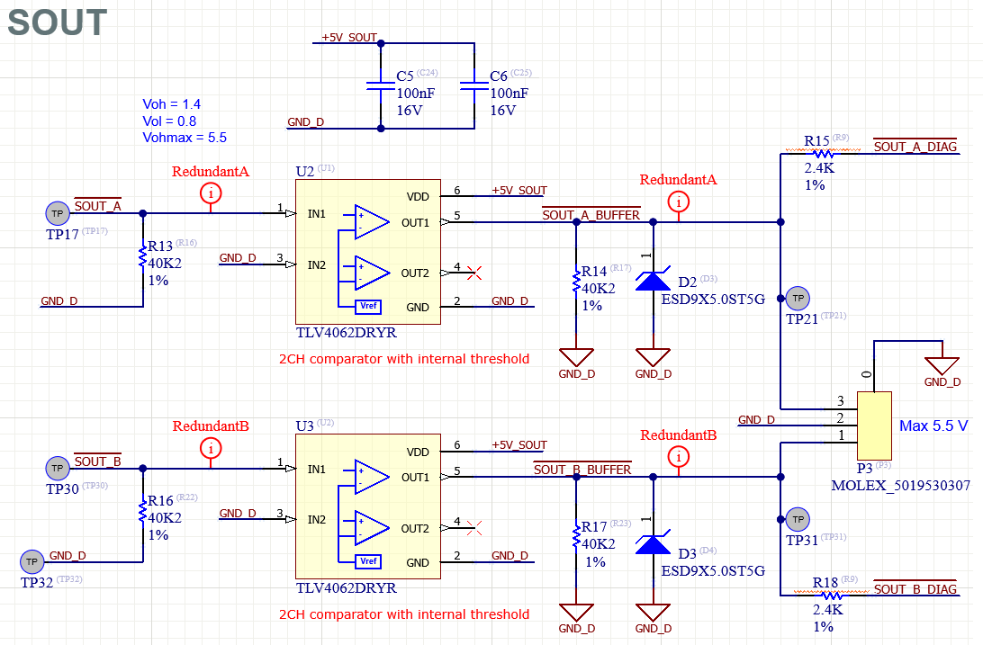
The SOUT signals originating from the drive shall include a mandatory 40.2 kΩ ±1% pull-down resistor to GND.
-
The minimum external impedance, including the mandatory pull-down resistor described above, shall be greater than 25 kΩ to ensure that the Safe Outputs behave as specified.
-
Any capacitance connected to the Safe Output shall be limited to less than 100 nF, as higher capacitance may increase the output reaction time.
-
In the event of an external fault condition, the maximum reverse voltage that may be applied to a Safe Output is 25 V. The SOUT circuits of a specific channel might be damaged when a reverse voltages lower than 25 V is applied but the rest of safety circuits will be protected.
-
The Safe Outputs are not intended to directly drive standard 3.3 V or 5 V logic inputs. Since the outputs only guarantee a maximum VOL of 0.8 V and a minimum VOH of 1.4 V, an external buffer is recommended to translate these levels into well-defined logic signals and ensure robust operation under all conditions.
-
The Safe Output diagnostic inputs SOUT_A_DIAG_INPUT and SOUT_B_DIAG_INPUT shall be connected to the corresponding buffered SOUT signals through a series resistor of 2.4 kΩ ±5%. This resistor limits the input current to less than 2 mA when the input voltage reaches 6.5 V.
The diagnostic connections are mandatory for proper system operation. If they are not used, the diagnostic inputs shall be pulled up to 3.3 V. However, in this configuration, the applicable safety requirements will not be fulfilled.
Let us consider a theoretical implementation in which the safe outputs (/SOUT_X) are used to drive an externally connected LED indicator. In this architecture, the /SOUT_X signals originate from the drive and are conditioned by the interface-board circuitry (a buffer). The resulting signals (/SOUT_X_BUFFER) are routed to the external connector to drive the LED load, while the diagnostic feedback signals (/SOUT_X_DIAG) are routed back to the drive to allow monitoring of the output state.
Feedback Interface
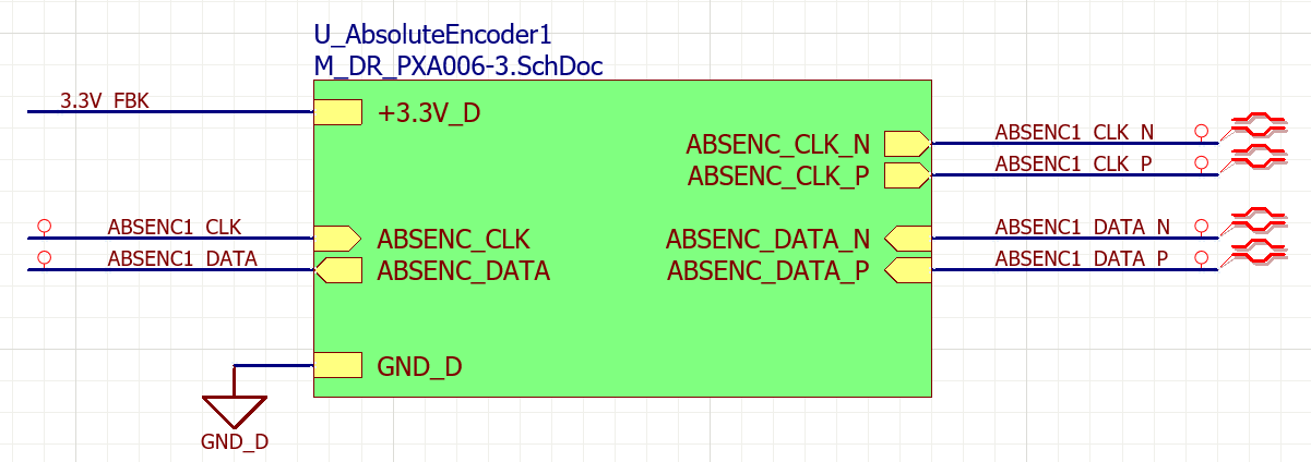
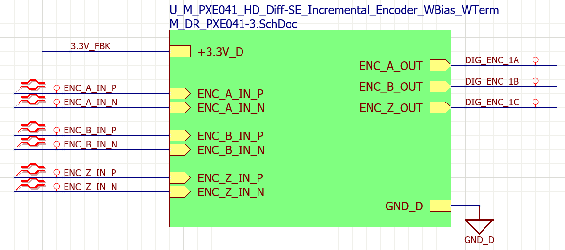
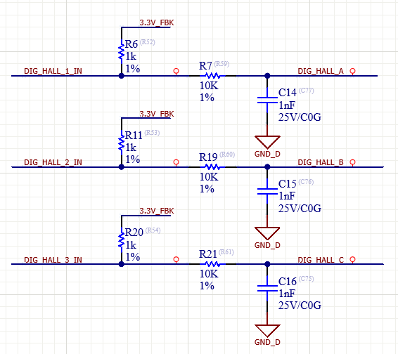
It is important to note that only specific feedback combinations are supported for use with Safe drives and guarantee the required safe-failure behavior. The Everest S Safe NET and Denali Safe NET drives are capable of providing advanced Safe Motion functions by utilizing two independent feedback devices to achieve redundancy. However, not all feedback configurations are supported in safety-certified applications. Additional information regarding the supported combinations is provided in the bellow table.
Safe drives can be integrated in systems consisting of either a motor alone or a motor coupled to a gearbox. In motor-plus-gearbox configurations, the feedback device mounted on the motor shaft is referred to as the redundant feedback, while the feedback device mounted on the gearbox output shaft is referred to as the main feedback. This arrangement allows the safety functions to monitor both the motor and the final mechanical output of the system.
In applications without a gearbox, both the main feedback and the redundant feedback monitor the same motor shaft, providing the redundancy required for the implementation of Safe Motion functions.
|
Feedback Combination |
||
|---|---|---|
|
Combination code → MotionLab selection |
Main feedback sensor |
Redundant feedback sensor |
|
FBC0 → No feedback |
- |
- |
|
FBC1 → Primary absolute and secondary absolute |
BISS-C BP3 - Port 1 |
BISS-C BP3 - Port 2 |
|
FBC2 → Primary absolute and incremental encoder |
BISS-C BP3 - Port 1 |
QEI |
|
FBC3 → Secondary absolute and halls |
BISS-C BP3 - Port 2 |
Digital Halls |
|
FBC4 → Incremental encoder and halls |
QEI |
Digital Halls |
A common strategy is to power the feedback transcievers from the 3.3V_SAFE_EXT output provided by the Safe drive. This dedicated supply rail can be used to power the feedback-interface circuitry while maintaining compliance with the system's safety architecture. Although its use is not mandatory, it represents a practical solution for circuits with a current consumption below 150 mA.
REMINDER: Always connect the 3.3V_FBK_SENSE pin to the supply net of the feedback sensors transceivers